주메뉴
-
Company

Company overview Greetings from CEO Management policy Quality policy Environmental policy Conflict Minerals Certifications Organization History Location
-
Business
-
Technology
Manufacturing
environment Assembly Visual Test Reliability Test -
R&D
Current patent status Electrical device Package Development Road map
-
Recruit
Personnel system Recruit announcement Right people Welfare FAQ on recruitment
-
Support
TECHNOLOGY
TECHNOLOGY
Die Attach
 > Tachnology > Assembly > Die Attach
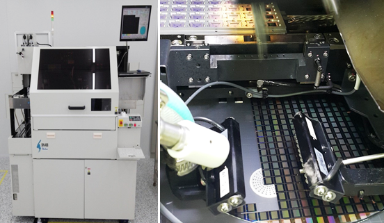
Equipment ability
| Min/ Max Die Size | 0.87~25mm |
|---|---|
| Thin die Capability | 75㎛ |
| Accuracy for XY and Theta | XY : ±25㎛ Theta : 0.5 |
| Camera Magnification Pre Bond/Bond Post Bon |
Pre Bond : 0.23~0.46 Option Bond Post bond : 0.15~0.87 Zoom |
| Wafer Size | 8inch ~ 12inch |
| Bond Force (Standard) | 15N |